Profile

Contact
Prof. Dr.-Ing. Jens Müller
Head of the Group
Telefon: +49 3677 69-2606
Prof. Dr.-Ing. Jens Müller
Head of the Group
Telefon: +49 3677 69-2606
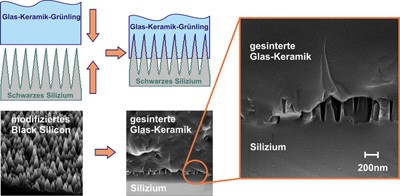
The combination of LTCC multi-layer technology and silicon technology in the "Silicon on Ceramics" process opens up a new dimension of system integration: silicon and circuit carriers are joined together before semiconductor production. The connection is made by sintering without the use of additives.
The technology is made possible by the use of pressure sintering and the use of a green film with an expansion coefficient adapted to that of silicon. The nanostructuring of the silicon surface prior to joining results in high tensile strengths around 5000 N/cm².
The result is a substrate with customer-specific back-wiring that can be processed in MEMS production lines.
Contact person: Dipl.-Ing. Michael Fischer
By using innovative technologies such as embossing, the conductor path thickness of ceramic circuit carriers made of Low Temperature Cofired Ceramics (LTCC) is significantly increased. This makes multilayer ceramics a cost-effective and reliable alternative to classic circuit carriers in power electronics. Deep trenches are stamped into the green foil and then filled with paste. In the fired state, this results in conductor paths up to 50 µm thick, which are characterized by a reduction of the electrical resistance and losses to one eighth compared to conventional, printed conductors. In addition to the reduced power loss, the good heat transfer and heat distribution in the ceramic ensure a high current carrying capacity. In addition, integrated components such as coils can be operated at a higher temperature with improved quality.
Contact person: Dr.-Ing. Heike Bartsch
Research cooperations
joint projects with industrial and research institutions at state, federal or European level
Contract research
Application-oriented research on behalf of industry with a research contract
Services (within the scope of the commercial operation (BgA))
Electrical characterization of dielectrics (metrological characterization of dielectric substrate materials up to approx. 1 GHz by means of S-paramter and RF I-V method)
Subracks (design and fabrication of thick film and LTCC modules)
Assembly technologies (assembly of microelectronic modules in SMD, Chip-on-Board and FlipChip technology)
Fault analysis in microelectronic assemblies (X-ray and ultrasound examinations for the detection of interconnection defects in microelectronic circuits, such as short circuits and interrupted connections)
Development and technology consulting (support in the selection of assembly and interconnection technologies as well as in the development of microelectronic assemblies)
Preparation of film templates on Agfa-OPF plan film