A research team at Technische Universität Ilmenau has succeeded in further developing a fundamentally new and very material-saving approach. This approach uses additive material synthesis for semiconductor metallization. The research results, developed in the Nanotechnology Group under the leadership of Professor Heiko Jacobs, follow up on prior publications on lateral nanobridge growth (Advanced Materials 2016, IEEE 2018, IEEE 2020) and open up news ways to connect metallization layers vertically, point-to-point, using a plasma jet process. The results were published in the January issue of Advanced Electronic Materials with cover.
Research
Advanced Electronic Materials Cover: Novel resource-efficient approach to semiconductor metallization
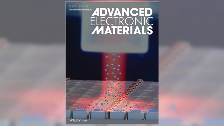
In their article on "Self-Aligning Metallic Vertical Interconnect Access Formation through Microlensing Gas Phase Electrodeposition controlling Airgap and Morphology", the scientists from the Nanotechnology Group at TU Ilmenau describe a completely additive approach to synthesize materials for the first metallization level in circuits. The material synthesis is based on directed electrodynamic transport of particles from the gas phase.
In this process, nanoparticles, i.e. assemblies of a few to a few hundred atoms with a diameter of 0.5-5 nanometers, are generated in nitrogen by spark discharge ignited by a high electrical field between two electrodes. The generated particles are transported to a pre-patterned substrate in a so-called plasma jet. "We are semiempirically investigating the influencing variables of the plasma jet, i.e. electrical power, gas flow and potential profile, in interaction with a structured substrate, in order to selectively deposit the smallest possible particles on the smallest possible area," Leslie Schlag, research associate at the Nanotechnology Group, explains.

The nitrogen ions from the plasma jet charge the substrate, and the particles can only grow a localized electrical connection from the substrate to the first metallization level because they are sorted into the substrate's potential funnels by the vast majority of nitrogen ions. "This can be thought of as a big exercise ball on a children's ball pool: If the big ball finds a depression or a hole, it moves in this direction," Leslie Schlag illustrates the deposition. Growth thus occurs centrally in vertical openings, where the charge of the nanoparticles can flow off, and without contact with the surrounding insulator. In the resulting and enclosing air gap, a relative permittivity of almost 1 is achieved, which is already very close to vacuum. "This corresponds to the minimum of all known materials and thus ensures very low interference capacities between neighboring vertical connections," Schlag says.
Resource-efficient additive material synthesis
While conventional semiconductor metallization is mostly subtractive, this novel material synthesis is completely additive. In conventional methods, more than 90% of the coated metal is removed after processing by etching. "This means that in conventional processes the wafers are first coated over their entire surface, but then the majority of the coating is removed again or etched away and ends up in the trash or has to be laboriously reprocessed, which is very expensive, especially in the case of rare but particularly conductive metals such as ruthenium or rhodium," Leslie Schlag explains: "In addition to this, the market for these materials is very tight, and most of them are extracted in platinum mines of Chinese corporations, but are then needed in Taiwan or the U.S. for semiconductor production or in the German automotive industry for exhaust gas catalytic converters. So, every consumer actively contributes to the shortage of the market."
Alternative to conventional methods of wafer metallization
In their work, the scientists have therefore also demonstrated the additive deposition of ruthenium and rhodium. These materials have the best electrical conductivity below 10 nanometers in dimension compared to other metals, but they are much rarer and therefore more expensive in their purest form than copper, gold, silver or aluminum. Subsequently, additive use is a very material-saving approach. "With this fundamentally new method, we are enabling an innovative approach that represents an alternative to conventional wafer metallization technologies," Schlag explains.
The research team's next goal is to increase the deposition temperature to also bring the electrical resistance of the structures to a marketable minimum and to reduce the currently demonstrated width of the electrical interconnect from 100 to 10 nanometers. "For the structure sizes shown, we had to rely on shape-beam electron beam lithography at IPHT Jena as a resource that enables faster processing of wafers with resolutions below 100 nm." Seven parameters were varied with each other and tested in more than 150 experiments, which required many substrate chips. On each chip there were additional sub-experiments in the form of geometry variations. "Now we are able to understand most of the influencing parameters and are confident that we will be able to fabricate the target 10 nanometer interconnect in a 50 nanometer vertical interconnect access using electron beam lithography in the laboratories of our university's Center for Micro- and Nanotechnologies."
Transport phenomena open up new fields of application
The published results were obtained within the framework of the projects JA 1023/6-1 and STA 556/6-1 funded by the German Research Foundation (DFG) under the title "Localized Transport from the Gas Phase", which can be considered as absolute basic research as they investigate any transport phenomena of particles of different size scales - metal particles, molecules, bacteria, fungal spores, pollen or even phages. During the experiments, all surrounding fields -current, E-field, B-field, and temperature - are manipulated both globally in the reactor and locally on the deposition substrate. "These transport phenomena are exploited to open up new applications, usually with a different goal at the beginning of the experiments, but as they progress they show that other applications can be opened up," Leslie Schlag explains: "Research in this field can therefore be seen as rather anti-disciplinary, as it encompasses everything and looks at the problem in its entirety. This is also what makes this research so charming."
The work was done in collaboration with researchers from the Leibniz Institute for Photonic Technologies IPHT Jena and the Institute for Nanotechnology and Correlative Microscopy INAM Forchheim and is available via the following link:
Contact
Leslie Schlag
Research Associate Nanotechnology Group