Scientists at TU Ilmenau have developed an unconventional method based on a nanometer-scale scanning tip to structure and study two-dimensional, semiconducting nanomaterials with the highest precision in a minimally invasive manner. The research results were obtained as part of a doctorate within the Research Training Group (RTG) "Tip- and laser-based 3D nanofabrication in extended macroscopic working areas" (3D-NanoFab) headed by Prof. Steffen Strehle and have recently been published in the renowned journal "Advanced Materials".
As a semiconductor material for computers, smartphones or solar technology, for example, silicon is usually used. However, as the performance requirements for modern electronics are becoming ever more stringent, new semiconductor materials for electronic components and the associated technologies must also be researched. Two-dimensional materials such as graphene are currently being discussed intensively as alternative materials.
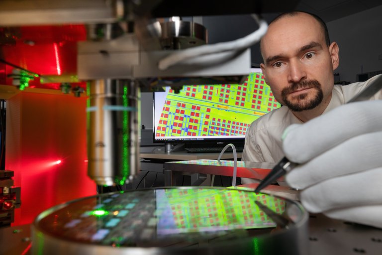
However, in order to realize their potential as ultra-thin materials for efficient electronics, i.e. only a few atomic layers thick, they must not only be produced, but also structured and functionally integrated into electronic architectures. As conventional microtechnologies can impair the materials and their properties, new technological hurdles arise. TU Ilmenau scientists have addressed these challenges in their latest research: The method they have developed for structuring two-dimensional materials is based on a nanoscale tip with a radius over 5000 times smaller than the diameter of a hair, which is guided over the surface of the material with the utmost precision, similar to atomic force microscopy. By applying a voltage between the material and the tip, the tip emits electrons with comparatively low energy and "bombards" the sample surface with highly localized electrons - i.e. exactly where the two-dimensional material is to be structured, i.e. brought "into shape".
Any surface pattern without measurable change in material

The scientists used flakes of the two-dimensional material molybdenum ditelluride (MoTe2) just a few atomic layers or nanometres thick, which they oxidized into water-soluble oxide with the help of electron bombardment and water molecules in order to subsequently remove it in a targeted manner. "Through the controlled movement of the tip and the associated local oxidation, we were able to create virtually any surface pattern without causing any other measurable changes in the two-dimensional material," explains Christoph Reuter, a second-generation doctoral student at the interdisciplinary Research Training Group (RTG) "3D-NanoFab". He carried out the research work as part of his doctorate together with Professor Steffen Strehle, spokesperson for the Research Training Group and Head of Microsystems Technology at TU Ilmenau, and Dr. Gernot Ecke, research assistant at the Nanotechnology Group.
The scientists used their method to produce an ultra-thin transistor from just three atomic layers of MoTe2 in order to inspire further research, for example in the field of innovative electronics, sensor technology or energy conversion: "We want to expand our method in the coming years and also use it for applications in the field of 'green' energy-efficient electronics," says Prof. Strehle: "The research results will also be directly incorporated into courses at TU Ilmenau in order to involve students, for example in the Mechatronics, Mechanical Engineering and Micro- and Nanotechnologies degree programs, in our research at an early stage."
More about the master programs offered at TU Ilmenau
About the Research Training Group 3D-NanoFab
The Research Training Group on tip- and laser-based 3D nanofabrication in extended macroscopic working areas has been funded by the German Research Foundation (DFG) since 2017 and enables young researchers to complete a doctorate at the highest level. As part of the structured research and qualification program, they are employed in three highly specialized research areas: the development of processes for production in the nanometer range, the control and regulation of fabrication machines for the high-precision positioning of processing tools and the metrological validation of production results.
Original publication
Reuter C, Ecke G, Strehle S (2024). "Exploring the Surface Oxidation and Environmental Instability of 2H-/1T'-MoTe2 Using Field Emission-Based Scanning Probe Lithography", Advanced Materials, 36, 2310887 (1-14), https://doi.org/10.1002/adma.202310887
Contact
Prof. Steffen Strehle
Spokesman Research Training Group 3D-NanoFab, Head of Microsystems Technology