Google Suche
Prof. Dr. rer. nat. habil. Thomas Hannappel
Fachgebietsleiter
Raum: Meitnerbau 1.3.106
E-Mail: thomas.hannappel@tu-ilmenau.de
Telefon: (+49) 03677 69-2566
Preparative and analytical work is devoted to the preparation of next generation, highly efficient solar cells and photoelectrochemical devices for water splitting and CO2 reduction in the form of thin epitaxial multi-layer systems of silicon, germanium, or III-V materials. Novel concepts and new routes of multi-junction devices are prepared applying the metal organic chemical vapor deposition (MOCVD) technique. The development of highly efficient solar cells and water splitting devices as well as fundamental issues of interfacial reactions, are guided by the insights gained from state-of-the-art powerful analytical tools, i.e. several methods of optical spectroscopy, in situ analysis, and surface science in ultrahigh vacuum.
Multi-junction solar cells are today’s most efficient solar cells. The growth process is controlled via optical in situ signals (such as reflectance anisotropy spectroscopy, RAS) allowing for systematic monitoring of the changes of the surface structure and for systematic improvements of the growth procedure and therefore, to control the interface formation. Here, critical interfaces, such as the III-V/Si(100) and the liquid/III-V heterointerfaces are targeted.
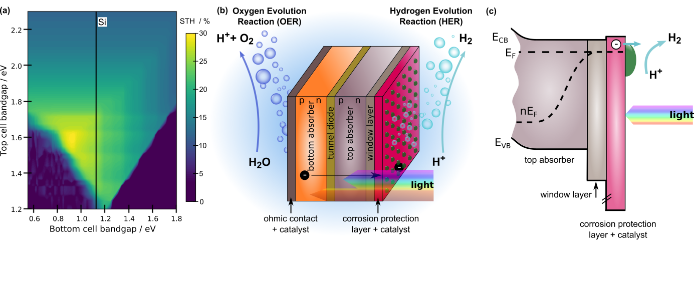
Hydrogen is a promising energy carrier to supply the energy demand of the world and to concomitantly reduce greenhouse gas emissions. Artificial photosynthesis enables solar-driven production of hydrogen through photoelectrochemical (PEC) water splitting. To split water into hydrogen and oxygen the PEC cell needs to generate a voltage larger than 1.23 V:
Anodic reaction: 2H2O → O2 + 4e- + 4H+
Cathodic reaction: 4H+ + 4e- → 2H2.
Including overpotentials, which are required to drive the chemical reaction, a photovoltage of about 1.8 V is needed. The solar-to-hydrogen (STH) conversion efficiency of a single junction absorber with such a high bandgap would be strongly limited due to optical transmission losses. These energy losses can be significantly reduced by the use of multi-junction (MJ) absorbers, in which subcells with different bandgaps are stacked on top of each other and absorb the sunlight in different spectral ranges. To date, III−V semiconductor (MJ) absorber structures prepared on germanium substrates enable the highest solar-to-hydrogen efficiencies in PEC cells [Nature Communications 6 (2015) 8286; ACS Energy Letters 3 (2018) 1795]. The costs of these PEC cells can be significantly reduced by substituting the Ge substrate with silicon. The combination of III-V semiconductors with a Si(100) substrate as an active bottom cell in a two-junction device, enables STH-efficiencies close to maximum, over 25%.
Such a tandem absorber device requires the preparation of ideal structures in all involved interfaces. A detailed understanding of the reactions at the semiconductor/electrolyte heterointerface is essential to design the semiconductor surface appropriately, reducing corrosion while maintaining an efficient charge transfer over the interface. In particular, the surface reconstruction of the InP(100)-based window layer, used as charge-selective contact, and its chemical reactions with the environment might impact the formation of charge-carrier recombination centers upon exposure to the aqueous electrolyte. Minimization of such states is crucial for achieving high STH-efficiencies. In realistic device configurations with a thin metal oxide corrosion protection layer and catalysts the energetic alignment will be crucial. Our research aims to understand how the surface electronic structure affects the energetics and dynamics of electronic charge transport, transfer, and recombination in the (near‑)surface region.
Samples with atomically well-ordered surfaces are transferred contamination-free from MOCVD to the PEC cell via a mobile UHV shuttle. The photoelectrochemical performance (such as linear sweep voltammetry and stability measurements) of samples as a photocathode for water splitting is measured in a three-electrode setup upon exposure to aqueous electrolyte. Optical spectroscopy such as reflection anisotropy spectroscopy (RAS) allows us to study morphologic changes of the surface in situ. Photoelectron spectroscopy enables us to probe changes of the electronic structure induced by the adsorbates, to understand the surface chemistry, benchmark the corresponding optical in situ signals and tune the interface design to minimize losses of the charge carrier transfer.
Two experimental setups in the group are dedicated to measuring time-resolved photoluminescence of semiconductor structures. Photoluminescence refers to the emission of light from an illuminated sample. The temporal dependence of the luminescence from a semiconductor can provide important information of material and interface quality of the semiconductor. The measurement can be either performed by correlated single-photon counting or by using a streak-camera system, both available in the group. The former is an extremely easy-to-use method and is routinely used to study a wide range of materials, while the latter provides the highest temporal resolution combined with high excitation power and spectral resolution.
Among various types of solar cells, MOVPE-grown triple-junction III-V compound semiconductors are today’s most efficient photovoltaic devices with conversion efficiencies exceeding 40%. A next-generation multijunction cell with four or more junctions and optimized band gaps is expected to break the present record efficiency surpassing the 50% mark. High band gap material combinations that are lattice matched to GaAs are already well established, but the required low band gap combinations containing a band gap around 1eV are still to be improved. For this purpose, we have developed a low band gap tandem (two-junction) solar cell lattice matched to InP. For the top and bottom subcells InGaAsP (Eg = 1.03 eV) and InGaAs (Eg = 0.73 eV) were utilized, respectively. A new interband tunnel junction was used to connect the subcells, including thin and highly doped layers of n-type InGaAs and p-type GaAsSb. The delicate MOVPE preparation of critical interfaces was monitored with in-situ reflectance anisotropy spectroscopy (RAS). After a contamination-free transfer, the RAS signals were then benchmarked in ultrahigh vacuum (UHV) with surface science techniques like low energy electron diffraction (LEED) and X-ray photoelectron spectroscopy (XPS). XPS measurements revealed that the sharpest InGaAs/ GaAsSb interface was achieved when the GaAsSb layer in the tunnel junction of the solar cell was grown on III-rich (2×4)- or (4×2)-reconstructed InGaAs(100) surfaces. The improved interface preparation had a positive impact on the overall performance of the tandem cell, where slightly higher efficiencies were observed for the cells with the III-rich-prepared tunnel junction interfaces.
The costs of the solar cell can be significantly reduced by substituting the expensive III-V substrate with inexpensive and abundant silicon. In a tandem absorber structures combining an active silicon bottom cell with a GaAs0.75P0.25 (1.73 eV) top cell could reach solar energy conversion efficiencies close to 45%. Commonly the lattice mismatch between Si and the top absorber is bridged via graded GaAs1-xPx buffer, which is grown on a pseudomorphic GaP nucleation layer. By applying strain-balanced multi-quantum-wells (MQW) in the top absorber the amount of As incorporated into the GaAsP metamorphic buffer can be reduced to 50% (2.05 eV) with predicted energy conversion efficiency of 42.6% (60-period stack of 5-nm-thick GaAs0.8P0.2 wells and 3-nm-thick GaP barriers) [B. Kim et al. Sol. Energy Mater. Sol. Cells 180 (2018) 303].
The top target layer with new lattice constant in the graded buffer must be fully relaxed and exhibit a low threading dislocation density to allow high performance of the lattice mismatched top absorber. The growth parameters, such as temperature, number of the graded buffers, their thickness and post-growth annealing procedure will have a significant impact the relaxation of each buffer and density of dislocations. In addition, the reactor conditions and growth parameters largely impact the As incorporation in each GaP matrix. For efficient growth control, the As/P content should be quantified in situ directly from the growth surface without additional surface preparation steps. We developed a simple empiric model to quantify the As/P content of individual GaAsP graded buffer layers in situ during MOVPE growth with reflection anisotropy spectroscopy, which eases GaAsP growth control significantly [O. Supplie et al., APL 2020 submitted].
Since strain-balanced MQWs include a large number of heterointerfaces, their sharpens and abruptness, the control of atomic content profile and the management of strain are crucial for growing structures as designed, in addition, very thin buffers must be achieved. The abrupt change of the atomic content at the heterointerface in the MOVPE reactors is mainly limited by slow As to P exchange at the surface. Additionally, undesired in-diffusion of group-V element into the subsequently grown buffer layer should be avoided. Therefore, the optimum gas-switching sequence and additional purge periods of annealing only under H2 carrier gas must be adjusted.
The in situ measured optical signals show whether desired bulk properties and a specific surface reconstruction have been realized in the MOCVD reactor. A direct relationship is established between a specific optical signal and the corresponding surface reconstruction. This strategy is successful with a unique experimental tool. The latter enables contamination free sample transfer from the MOCVD reactor to ultra-high-vacuum. Thus, signals like LEED, UPS, XPS, AES, STM images, FTIR, and again RAS are measured in ultra-high-vacuum that characterize the specific surface reconstruction.
With increasing experience and know-how in this field optical fingerprint signals have been established also for buried interfaces. Easier to handle and more cost effective III-V solar cells can be realized by depositing III-V materials on Ge- or rather Si-wafers. Current estimates indicate a competitive cost level for multi-junction III-V cells with conversion efficiencies towards 50 percent if they are employed at concentrated sunlight.
Example: III-V on silicon
There is a strong scientific and technological interest in the realization of III-V semiconductor heteroepitaxy on silicon substrates, in particular, by applying the metal-organic vapour phase epitaxy MOVPE(1) technique for industrial scalability. The integration of optoelectronic devices such as high-efficiency solar cells on Si100(1) substrates requires a significant reduction of the defect concentration induced by the III-V on silicon heterointerface.
However, major challenges have to be met at the III–V/Si heterojunction: crucial issues are differences in lattice constants and thermal expansion coefficients as well as the formation of the heterovalent (polar-on-non-polar) interface necessitating a suitable substrate preparation prior to heteroepitaxy. New defect mechanisms – typically not observed in III–V homoepitaxy – arise from the interface with the Si(100) substrate and need to be controlled to achieve defect concentrations suitable for applications in advanced optoelectronic devices.
MOCVD Preparation of III-V materials
Metal Organic Chemical Vapor Deposition (MOCVD) or Metal-Organic Vapor Phase Epitaxy (MOVPE) is a widely used method for preparing epitaxial structures by depositing atoms on a wafer substrate. It is utilized for a broad variety of applications in industry and research. The principle of MOCVD is quite simple. Atoms are deposited by decomposing organic molecules (precursors) while they are passing over the hot substrate. The undesired remnants are removed or deposited on the walls of the reactor. III-V semiconductors of high purity and structural order are prepared via MOCVD.
The group operates an AIXTRON-200 MOCVD reactor.
It holds a German patent for the specific protocol of contamination-free sample transfer into ultra-high vacuum (UHV). The sample can be transported in a mobile UHV chamber and transferred into any other desired UHV chamber, provided the latter is equipped with an appropriate load-lock port. So-called alternative precursor molecules are preferred since they are less poisonous and permit sample growth at lower temperatures than conventional precursors.
Characterization of III-V materials, see below methods
In situ reflectance anisotropy spectroscopy
Sample growth is monitored in the MOCVD reactor with Reflectance Difference/Anisotropy Spectroscopy (RDS/RAS). RDS is a normal incidence reflectance technique probing the anisotropy that arises at a reconstructed surface. RDS measures the difference in the normal-incidence reflectance rx and ry of linearly polarized light directed onto the sample's surface. The signal is normalized to the total reflection <r>. The basic principle of RDS is the measurement of the complex reflectance anisotropy rx-ry/<r>, caused e.g. by the reduced symmetry of the reconstructed surface of a cubic crystals.
The group measures RDS signals of MOCVD-prepared surfaces down to 20K, in particular clean and well-ordered III-V (100) and (111) surfaces.
Apparatus for investigating metalorganic chemical vapor deposition-grown semiconductors with ultrahigh-vacuum based techniques
An apparatus has been developed for the transfer of a sample from a metalorganic chemical vapor deposition (MOCVD) reactor to an ultrahigh-vacuum (UHV) chamber without introducing any contamination. The surface of the sample does not change during transfer as is borne out by the identical reflectance difference (RD) spectrum measured first in the MOCVD reactor, i.e., in situ, and afterwards again in the UHV chamber. Making use of the earlier apparatus a semiconductor can be grown in the MOCVD reactor and can afterwards be investigated with any desired tool of surface science, in particular also those that require UHV. All the data collected in UHV can be identified with the RD spectrum measured already in the MOCVD reactor. Several examples are presented here for data collection in UHV on III–V semiconductors grown in the MOCVD reactor. They illustrate the ease and reliability of the here described apparatus for contamination-free sample transfer. Signals are presented in particular for the genuine MOCVD-grown P-rich seemingly (231)/(232)InP(100) reconstructed surface that until now can only be investigated in UHV if one makes use of the sample transfer system described in this article.
Methods of Surface Science
Research topics
Services offered to companies:
Special equipment:
The sophisticated multi-tip scanning tunneling microscope (MTSTM) offers the possibility to electrically characterize planar, but especially structured semicunducting components. By using an equipped scanning electron microscope (SEM), four independently movable tungsten tips can be positioned with a high spatial resolution and corresponding I-V characteristics can be recorded. By changing the distance between the potential tips, the recorded IV-curves can then be used to generate a spatially resolved resistance and a dopant profile.
The charge-separating contacts required for opto-electronic components can thus be specifically investigated. Optical measuring methods such as electron beam induced current measurement (EBIC) or the illumination of the pn-junction by additionally incorporated fibers, where the latter provides an access to the fill factor and allows the qualitative evaluation of the charge separating junction.
Possible questions that could be addressed with the MTSTM are:
· detailed understanding of the dopant incorporation,
· the conduction channels at different doping levels and
· the function of charge-separating contacts in semiconducting structures.
Example: III-V nanowire structures
Due to the high surface-to-volume ratio of nanowire structures, they are particularly sensitive to changes in their surface. The MTSTM provides a unique opportunity to electrically investigate single, upright standing NWs on the nanoscale. The unique connection of the MTSTM to the MOCVD growth equipment by means of a UHV shuttle, as described above, allows the contamination-free transfer of MOCVD grown nanowires and their subsequent examination in the MTSTM. Conclusions can be drawn about the charge carrier transport pathways in the core and on the surface as well as their interaction with changed doping.
The group operates a SPECS Aarhus 150 scanning tunneling microscope. Samples are routinely transferred contamination-free from the MOVPE environment to the STM employing a mobile UHV chamber. By STM, the atomic surface structure is investigated, revealing in particular the step structure, the surface reconstruction and defects at the surface. Numerous MOVPE-prepared semiconductor surfaces have been studied this way and results have been correlated with other surface science methods, enabling crucial improvements of surfaces and interfaces for solar energy conversion.